Skip to the content Skip to the Navigation

茨城大学 半導体研究室 講師 坂根駿也

  • Profile
  • Research
  • Conferences
    • Domestic Conferences
    • International Conferences
  • Research Achievements
    • Papers
    • Books
    • Fundings
  • 日本語
  • 産業財産権
  • 受賞

ナノ構造・薄膜を用いて新材料を創成する

分子線エピタキシー(MBE)法による薄膜作製を基軸に、熱を電気に変える薄膜熱電変換材料や、赤外受光材料の研究に取り組んでいます。
研究内容を見る

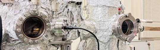
分子線エピタキシー法による薄膜成長技術

高品質なエピタキシャル薄膜を成長します。

Shunya Avatar

Shunya Sakane
Graduate School of Enginerring Science, Ibaraki Univeristy, Assistant professor

●Databases at Ibaraki Univeristy

●researchmap

●Semiconductor Lab's HP (Prof. Udono)

NEWS

  • A paper on the Cu2Se/PNIPAM catalyst has been published in Materials Today Communications!2026-10-16
  • I attended the 87th Autumn Meeting of the Japan Society of Applied Physics.2026-09-15
  • I attended the TSJ20262026-09-15
  • 令和8年度「大学× 国研×企業連携によるトップランナー育成プログラム」育成対象者(第6期TRiSTARフェロー)に認定されました!2026-07-15
  • I participated in the Summer School on Silicide-based Semiconductors2026-07-15

NEWS List

  • 日本語

Copyright © 茨城大学 半導体研究室 講師 坂根駿也 All Rights Reserved.

Powered by WordPress & Lightning Theme by Vektor,Inc. technology.

MENU

Language

  • English
  • 日本語
  • Profile
  • Research
  • Conferences
    • Domestic Conferences
    • International Conferences
  • Research Achievements
    • Papers
    • Books
    • Fundings
  • 日本語
  • 産業財産権
  • 受賞